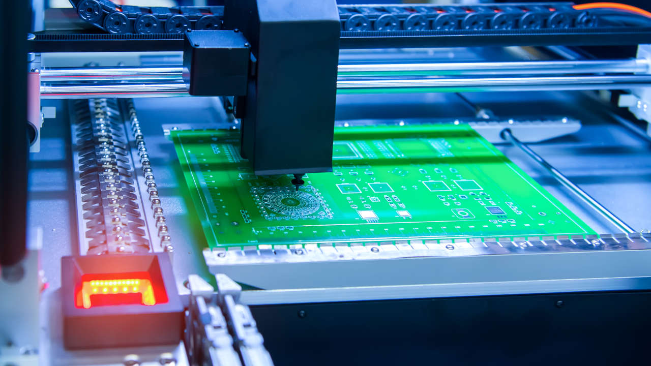
PCB design enablement is where innovation meets feasibility. Unlike standard boards, advanced custom designs address unique performance goals, mechanical constraints, or integration challenges that off-the-shelf layouts cannot accommodate. These capabilities are essential in high-stakes sectors where every millimeter of space and every signal matters.
We collaborate closely with your design engineers and trusted partners to ensure layouts meet your application requirements. Through design for manufacturability (DFM) feedback, assembly insights, and signal integrity support, we help optimize designs for functionality, manufacturability, and performance.
Whether supporting a new layout, optimization, or redesign, we partner with your team using advanced ECAD tools and IPC-compliant practices to help reduce iterations and accelerate time to market. From high-speed digital interfaces and RF considerations to thermal control and stack-up review, we ensure your PCB is ready for seamless assembly.
PCB design enablement means supporting the creation of circuit boards that meet your product’s unique electrical, mechanical, and regulatory needs. Our role is to strengthen your engineering vision by addressing critical factors like signal integrity, power distribution, thermal behavior, and manufacturability.
This approach is crucial when off-the-shelf solutions fall short, especially in space-constrained or high-performance applications. Tailored support helps ensure better performance, integration, and long-term reliability, setting the stage for smooth PCB assembly execution and compliance.
Foxtronics EMS helps OEMs and product developers bridge the gap between complex design intent and reliable, high-quality assembly.
Successful PCB design enablement begins with collaboration. We work closely with your engineering team to translate requirements into manufacturable layouts, balancing electrical performance, mechanical fit, and production feasibility.
We help you go beyond standard specifications, whether working with unconventional form factors, integrating multiple technologies, or addressing complex electrical and mechanical challenges. Our focus on cross-functional input, real-time DFM feedback, and simulation support helps minimize design iterations and accelerate launch timelines.
Before fabrication, we support validating every design element to ensure it meets performance, reliability, and cost objectives. This includes stack-up reviews, signal integrity assessments, and thermal analysis, all aligned for a seamless transition into prototyping and assembly.
High-speed and high-frequency PCB layout support through design partnerships
Mixed-signal design guidance with isolation and partitioning
Multilayer, HDI, and rigid-flex stack-up review
Differential pair and impedance-controlled routing support
Thermal analysis and heat management guidance
EMC and EMI mitigation strategies
DFM and DFT feedback
Support for custom footprints, components, and interconnects
PCB design enablement is essential in advanced product development, especially where standard solutions fall short. We support a wide range of high-performance applications across critical industries:
PCB design enablement is not just about reviewing CAD files. It is about understanding your performance needs, production realities, and long-term goals. We partner directly with your engineering team and external experts to ensure your layout not only meets today’s requirements but also supports future scalability.
Whether you are building a compact wearable, a high-speed data processor, or a rugged industrial controller, we help bridge the gap between your concept and a manufacturable, reliable design.
What We Offer
A collaborative enablement approach with your engineering team or trusted design partners
Full-stack integration support, including design feedback, simulation insight, and in-house prototyping
Thorough manufacturability and testability reviews
Proven success across regulated industries such as medical, defense, and aerospace
Fast turnaround and first-time-right assembly philosophy
Designing a custom PCB involves balancing electrical performance, space, thermal demands, and cost. Below are answers to common questions about how we approach these challenges and support you through the design process.
A custom PCB is purpose-built to match specific product or system requirements, such as unique dimensions, signal routing needs, environmental resistance, or non-standard components, rather than relying on generic board templates.
Absolutely. We assist in creating balanced multilayer stack-ups and provide impedance control calculations critical for signal integrity and EMI performance.
We work with all major ECAD formats such as Altium, Eagle, OrCAD, and KiCAD, and can also support Gerber, ODB++, and IPC-2581 output files.
Yes, we provide simulation services including signal integrity (SI), power integrity (PI), thermal analysis, and EMI/EMC modeling as part of our design validation process.
We apply rigorous DFM and DFT checks at each stage of the design process, incorporating feedback from our manufacturing teams to avoid costly rework or redesign.
Definitely. Whether it’s enhancing signal performance, reducing EMI, or shrinking board size, we can rework your existing layout for improved performance and manufacturability.
We welcome collaboration. Our team can work closely with your engineers during each phase, from schematic capture and layout to prototype feedback and production handoff.